COSINC-CHR
The Characterization (CHR) facility within COSINC provides access and training on state-of-the-art instrumentation utilizing a wide range of materials characterization techniques, including Field-Emission Scanning Electron Microscopy (FE-SEM), conventional SEMs, Atomic Force Microscopy (AFM), Scanning Tunneling Microscopy (STM), Focused Ion Beam (FIB)-SEM and capabilities such as Energy Dispersive Spectroscopy (EDS) and Electron Backscatter Diffraction (ESBD). In addition, the lab includes a sample preparation room for users.
List of equipment that may be scheduled. Users will require a PPMS account to be able to reserve an instrument. See details at resource scheduler.
COSINC-CHR
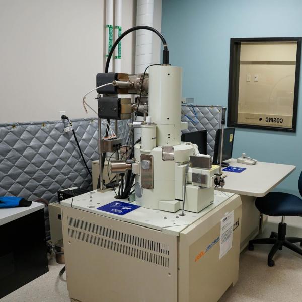
Field Emission Scanning Electron Microscope
Model: JEOL JSM-7401F
Cold field emission gun, magnification possible up to 200kx, two secondary electron detectors

Scanning Electron Microscope
Model: Hitachi SU3500 VP SEM
W-filement SEM with EDS and EBSD, variable pressure modes

Focus Ion Beam
Model: FEI Nova 600i Dual Beam
Dual beam system (Ga FIB + FESEM - thermal field emitter), Multiple gas injector system for deposition (Pt and SiO2), pc controlled nm resolution manipulator, TEM sample preparation

Atomic Force Microscopy
Model: Nanosurf DriveAFM
Tip-scanning, scan field sizes up to 90 µm, electrical/magnetic/mechanical properties measurements, STM capability

UV-VIS-NIR Spectrophotometer
Model: Shimadzu UV3600i with MPC-603A
Multi-purpose large-sample compartment, refelctance and transmittance measurements at several angles, from 190 nm to 3200 nm
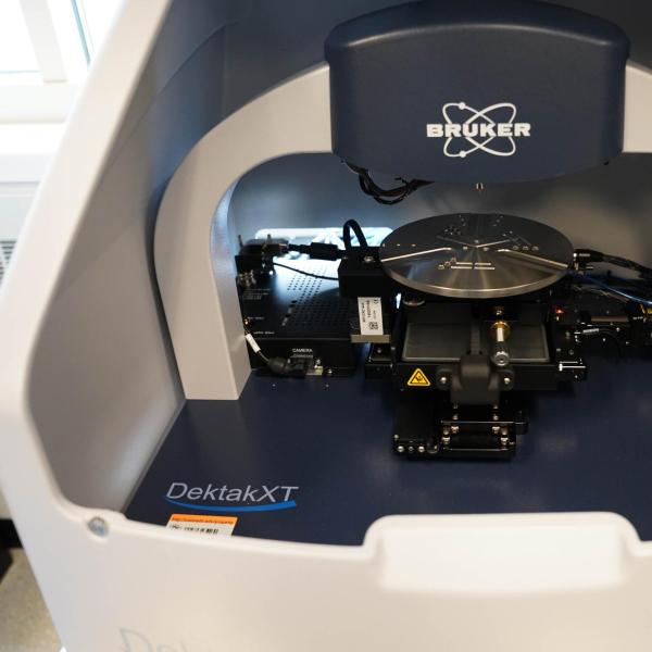
Surface Profilometer
Model: Bruker DektakXTA
Measurements repeatability of 0.4 nm for step heights measurements

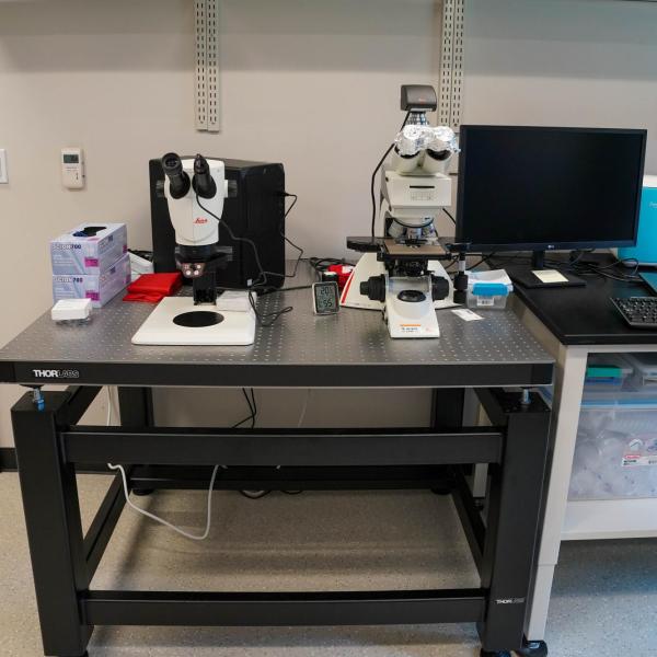
Optical Microscope
Model: Leica DM2700 Upright Materials Microscope
Transmission/refecting modes, white light LED illumination, bright field and dark field observation

Stereomicroscope
Model: Leica S9 series Greenough
9:1 zoom with magnification 6.1x-55x, 10x, field of view of up to 37.6 mm
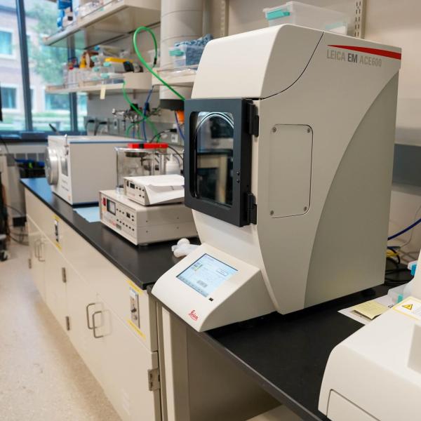
Sputter Coater/Carbon Coater
Model: Leica EM ACE600
Sputtering with TMP vacuum (Au and Pt targets available), carbon thread evaporation, only for EM applications

Critical Point Dryer
Model: Leica EM CPD300
Drying delicate samples for SEM applications and preserve the surface structure of specimen

Tabletop SEM
Model: Hitachi TM-4000PlusE-2 with EDS
Integrates ease of use with optimized, high-quality imaging in a compact design
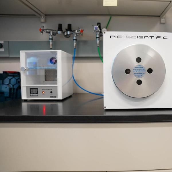
Plasma Cleaner
Model: PIE Scientific Tergeo-Plus
Automatic plasma cleaner with quartz chamber, enhanced chemical resistance and reduction of alkali impurities

X-ray Photoelectron Spectroscopy
Model: Kratos Axis Supra XPS Surface Analysis System
Surface sensitive technique to analyze composition of sample and chemical shift information within the first 10 nm. Equipped with monochromated X-ray gun (Al and Ag anodes) and UV Photelectron Spectroscopy (UPS) He lamp. Equipped with Gas cluster ion source (GCIS, Mininbeam 6), operates in both Arn+ cluster and Ar+ monatomic modes, suitable for sputter cleaning, depth profiling organic, inorganic and metallic films

Low Energy Ion Scattering Spectroscopy
Model: Iontof QTac100 High Sensitivity LEIS system
Provides the elemental composition of the outer atomic layer of surfaces. Includes small spot analysis, surface imaging, static and dynamic depth profiling.

X-ray Diffraction
Model: Rigaku SmartLab 9kW
Provides a variety of parameters including phase identification, lattice parameter, crystallite size, strain, and texture quantification, electron density and layer thickness quantification, and epitaxial quality for a variety of bulk or thin film samples. X-ray diffractometer has both Cu and Mo Ka targets. Supports transmission and reflection measurements including powder diffraction, thin film diffraction, X-ray reflectivity, rocking curve, and GI-WAXS. Air-free sample holders are available.
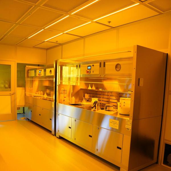
COSINC-FAB Clean Room
The Fabrication (FAB) cleanroom facility, within COSINC provides access and training on various state-of-the-art instrumentation in lithography, mask-making, thin-film deposition, thermal and wet processing and etch systems. The lab accommodates a wide variety of fabrication projects and sample materials for applications in areas ranging from electronics, optics, material science to chemistry and medicine.
List of equipment that may be scheduled. Users will require a PPMS account to be able to reserve an instrument (see details under resource scheduler).
COSINC-FAB Clean Room
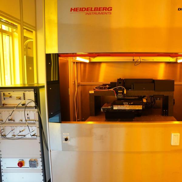
Heidelberg Laser Writer
Model: DWL 66FS
The Heidelberg DWL 66FS is a laser lithography system capable of writing up to 8 x 8 inches and direct writing patterns on wafers, with critical dimension down to 1 µm. Readable formats are DXF, HPGL, Gerber, GDSII, or CIFI
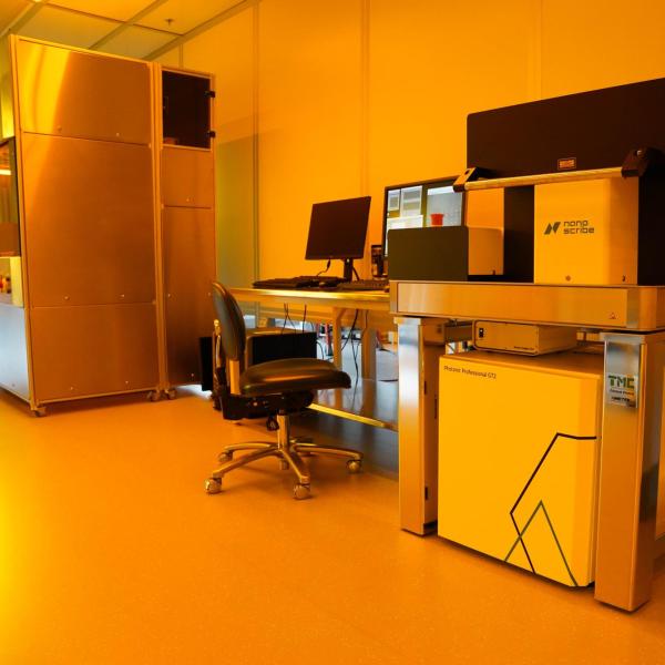
Nanoscribe 3D Nanoprinter
Model: Photonic GT2
Nanoscribe's Photonic Professional GT2 uses Two-Photon Polymerization (2PP) to produce filigree structures of nearly any 3D shape by high-precision 3D printing: crystal lattices, porous scaffolds, naturally inspired patterns, smooth contours, sharp edges, undercuts and bridges are all manufacturable with high resolution. More than a thousand successful research projects by Nanoscribe customers and system users are evidence of the power of two-photon lithography.
Printing technology: Layer-by-layer Two-Photon Polymerization
Minimum XY feature size: 160 nm typical; 200 nm specified*
Finest XY resolution: 400 nm typical; 500 nm specified*
Finest vertical resolution: 1,000 nm typical; 1,500 nm specified*
Layer distance: variable, 0.1 – 5.0 µm*
Maximum object height: 8 mm*
Build volume: 100 × 100 × 8 mm³ *
Minimum surface roughness Ra: ≤ 20 nm*
Max. scan speed: from 100 to 625 mm/s*
* Values may vary depending on the Solution Set, objective or photoresin in use

Thermal Evaporator
Model: CVC SC-300
Two boat thermal evaporator which can accomodate boats ranging from 1.875" up to 4 inches. Horizontal stage does not rotate. Base pressure ranges from 5e-6 to 2e-5 via cryopump. Manually opperated power suply, shutter, and crystal quartz monitor. This chamber is open to most materials with little restrictions.

Mask Aligner
Model: Karl Suss MJB3
Contact mask aligner for patterning 2 inch wafers and wafer pieces. Accepts 4x4 inch photomasks. CDs down to 1 micron possible (2.5 micron or larger reccomended) and alignement tolerences < 1 micron is achievable. Hard contact, soft contact, and vacuum mode (vacuum mode only avalable for small substrate pieces). 5x, 10x, 20x objectives for topside alignment.

Asher (O2 Plasma)
Model: March Jupiter 3
300 Watt, 13.56 MHz, Oxygen plasma asher used for wafer descumming and surface prep with pressures typically ranging from 100-500 mT. Chamber has a 5 inch diameter lower electrode that can accomodate wafer pieces and full wafers up to 4 inches.

Apex ICP Chlorine Ethcer
Model: PlasmaTherm Shuttle Lock
Inductively coupled plasma tool plumbed with Cl2, BCl3, O2, CHF3, Ar, N2. This tool is currently restricted to III-V materials. Mechanical clamp accepts 4 inch wafers, smaller wafers or wafer pieces can be mounted to 4 inch carrier wafers. He backside cooling is available.
ICP generator: 2000 W at 2 MHz
RF generator: 600 W at 13.56 MHz
Platen temperature 20C to 40C
Chamber Temp 20c to 100C

Spinner Coaters
Model: Laurell
2 Laurell spin coaters for coating substrates with photoresists and resins. One spinner is dedicated to e-beam lithography resists while one is open for general use. 100-6000 rpms are capable with multi step programming. Solvent spinning is not allowed.
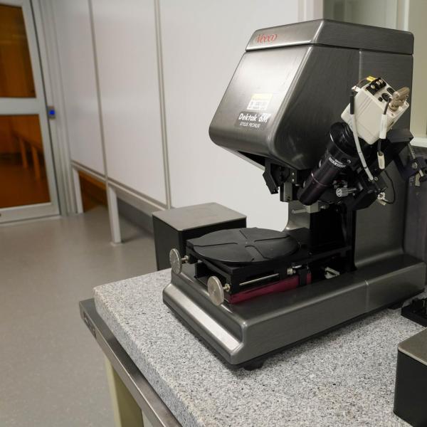
Profilometer
Model: Dektak 6m
Stylus profilometer capable of measuring features 50 nanometers to 100 microns. 12.5 micron stylus radius with adjustable stylus force.

Microscope
Model: Olympus AX70
Optical microscope with 5x, 10x, 20x, 50x, and 100x objectives. Bright field, dark field, and backside imaging modes. 10x magnification on eye pieces. AmScope camera connected to an imaging pc for saving color images and video at 2048x1536 resolution. Calibrated measureing using the imaging software.

Atomic Layer Deposition
Model: Beneq TFS-200
Thermal ALD used to grow oxides of Ti, Al, Sn, and Zn, and combinations thereof using the associated metal precursors and either water (precursor bubbler) or ozone (generated on the tool).
Precursors include Trimethylaluminum (TMA), Water, Titanium tetrachloride (TTC), Diethylzinc (DEZ), (Tetrakis)dimethylamido tin (IV) (TDMA-Sn), and Oxygen/Ozone

Reactive Ion Etcher
Model: PlasmaTherm Vision 320
Anticipated install date winter 2023. RIE chmber designed for low to medium density plasmas. 12 inch diameter platten can accomodate full wafers or wafer pieces, maximum wafer size 280 mm. 600 watt, 13.56 MHz, RF plasma. Temperature control of lower electrobe between 5 and 40 C ± 3 C. Optical emission endpoint etch monitoring for endpoint detection and allowing automated process control of target etch depth repeatable to < ± 2%
(run-to-run). Plumed with CF4, CHF3, SF6, O2, N2

Thin-film Deposition system
Model: Angstrom Engineering
Anticipated install date spring/summer 2024.
Combination electron beam evaporator and sputter tool.
6x7cc pocket e-beam evporatoration with a 6 kW (10 kV - 600 mA) solid state power supply. Programmable sweep pattern and rate control.
Two 3-inch sputter targets.
1.0 kW solid state pulsed DC power supply capable of running in DC or pulsed DC mode, 0 - 100 kHz pulse frequency, 0 - 800 V | 0 - 2.5 A.
600 W RF Power Supply and Matching Network, 13.56 MHz power supply with automatic matching network.
Rotating substrate stage with temperature control from ambient to 600C, height control, and up to 100 W RF bias

EBeam Lithography
Model: Raith EBPG5150plus
Anticipate install date summer/fall 2024. 100 kV Electron Beam,125 MhZ pattern generator, linewidth < 8 nm, stitch accuracy < 8 nm, overlay accuracy < 5 nm, max, field size of 1.048 mm
Solvent/developer bench
Model: Kinetics
2 stainless steel solvent processing benches are available for wafer prep, cleaning, and lithographic developing and resist stripping. Both benches have hot plates, DI water sinks and sprayers, and nitrogen guns available. The left bech also has a heated sonnicator with two power levels and can hold 250 mL beakers.
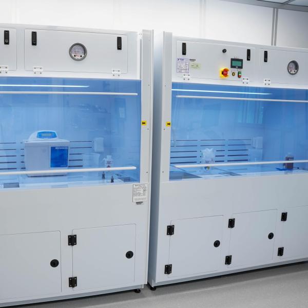
Corrosive bench
Model: Kinetics
2 polypropylene benches used for wet etching using acids and bases. No piranha or HF allowed, however the shelf stable nanostrip is allowed and stocked as a safer piranha alternative. Both benches are equiped with DI water sinks and sprayers as well as nitrogen guns.